So lets just jump into the fun stuff – spectrum plots! First, we will start off with our baseline. This is the codec shield playing back a 10 bit, 1024 sample sinewave from its internal memory. The horizontal axis is frequency, and the vertical axis is the amount of energy at that frequency. You can see a strong peak at 1kHz, which is our test tone, and a large hump around 30Hz, which is a result of low frequency noise and DC offset (0Hz).

Figure 1 – ADC spectrum analysis for codec shield playing back a 10b look-up table.
This test tone is the equivalent of near perfect ADC with 10 bit depth, and shows the codec shield’s contribution to the noise spectrum. The 1kHz signal is a few dB stronger than in the following plots, as the look-up table covered the full amplitude range, and our ADC samples only went to 4V out of a possible 5V. It also has much lower noise and distortion components than the ADC playbacks, giving it an effective number of bits (ENOB) of 9.8.
These next screen shots represent the ADC samples. They are all taken with a 1kHz tone at 4Vpp, 2.5V offset (Arduino running at 5V). The ADC samples were played out via the codec shield at a rate of 7.35ksps, with the exception of the 125kHz ADC clock setting, as this was too slow, and needed to be played back at 4.009ksps. The 125kHz tests also used a 500Hz tone to ensure the third harmonic was captured. Notice that the noise is flatter (although higher) than for the look-up table, as the finite samples of the look-up table caused the noise to occur more prominently at certain frequencies related to its repetion rate.

Figure 2 – ADC spectrum analysis (clocked at 125kHz – first sample mode, 2kHz bandwidth)
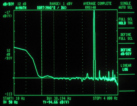
Figure 3 – ADC spectrum analysis (clocked at 250kHz – first sample mode)
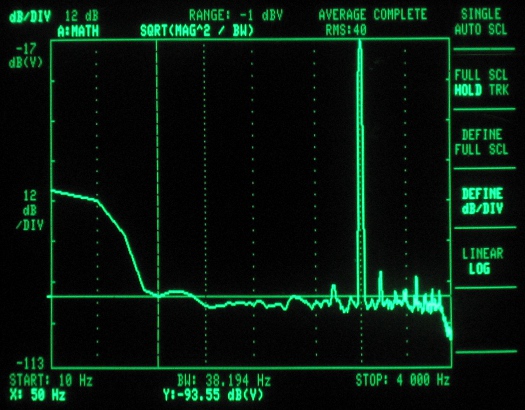
Figure 4 – ADC spectrum analysis (clocked at 500kHz – first sample mode)
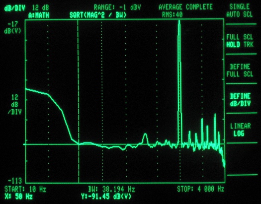
Figure 5 – ADC spectrum analysis (clocked at 1MHz – first sample mode)
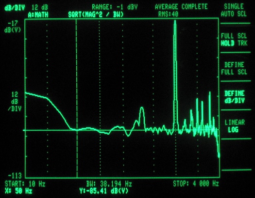
Figure 6 – ADC spectrum analysis (clocked at 2MHz – first sample mode)
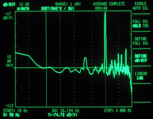
Figure 7 – ADC spectrum analysis (clocked at 4MHz – first sample mode)
All of these plots were taken in first sample mode, as the codec shield runs on its own timed interrupt, setting the sample rate. What happens if you don’t do this? Check out the plots below, which show the frequency modulation you get from clock jitter, greatly raising the noise floor. You can see the modulation depth varying with the ADC clock period.
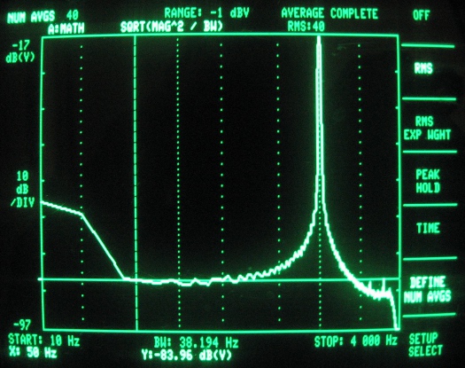
Figure 8 – ADC spectrum analysis (clocked at 125kHz – single sample mode)
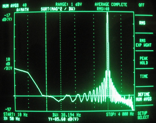
Figure 9 – ADC spectrum analysis (clocked at 250kHz – single sample mode)

Figure 10 – ADC spectrum analysis (clocked at 500kHz – single sample mode)
Bit-Depth Calculations
To calculate the effective number of bits (ENOB), we need to know 3 things: (1) the signal level, (2) the noise floor, and (3) the total bandwidth of the noise floor. This will allow us to calculate the signal to noise ratio (SNR), which is, as it sounds, the signal level divided by the total noise level. From there we use the following formula to calculate the ENOB:
ENOB = (SNR – 1.76dB)/6.02dB
Basically, for each additional data bit you double your range (2 bits gives 4 levels, 3 bits gives 8, and so on), giving you 20log(2) = 6.02dB more SNR per bit. The 1.76dB compensates for the fact that the noise floor is not a sine wave – it takes discrete steps for each bit. So its relative energy level is different from that of the input signal. For further reading on the derivation of this formula, check out this great app. note on ENOB from Analog Devices. They also have one explaining sigma-delta converters that is really good.
For our application, we used 3.8kHz as the total bandwidth, as the codec shield has a -60dB digital filter just past the Nyquist frequency, which explains the sharp cut-off in the plots. We approximated a flat response for the noise floor, and eyeballed the level with the spectrum analyzer’s markers. Multiplying the noise floor by the square root of the bandwidth gives the total noise energy. The square root is used because the spectrum analyzer displays in unts of dB per square root Hz.
The signal level was measured using the marker, and multiplied by its thin slice of bandwidth. And since we were only driving the input with a 4V signal (out of a possible 5V), we added 1.9dB (20log[5/4]) to reflect what the theoretical maximum would be for a full scale input. Since both values are in dB, we subtracted the noise from the singal, giving the SNR. The ENOB was then calculated using the formula above.
Oversampling
Although the noise floor increases with ADC clock frequency, you can take more samples per unit time. So there is the possibility of actually getting a better signal from a worse SNR via oversampling. Oversampling averages out the noise, but adds your signal, giving you an SNR increase equal to the square root of the number of averages. For example, if you run the ADC at 500kHz, you can take 4 times as many samples than if you run at 125kHz, giving a factor of 2 improvement (square root of 4). This is equal to a 6dB increase (20log[2]), giving 1 extra effective bit to your sample.
Although oversampling works as expected for reducing the noise floor, it quickly runs into trouble as the ADC distortion increases. This is because the distortion artifacts are correlated to the signal, and therefore add just as the signal adds. So, even though the noise floor will drop, the distortion will stay the same level. And, for ADC clock frequencies above 500kHz, the distortion is a significant portion of the noise.
Maximum Frequency
The above information gives the maximum usable ADC clock frequency as 4MHz, but what is the highest frequency you can sample? The limit to this is the set-up time on the S/H capacitor, which we measured as 500ns (1us if the MUX capacitor has changed). At 4MHz a clock cycle is 125ns, so the 2 clock cycle S/H capacitor charge time in free running mode is a bit short. In first sample mode you get 2.5 clock periods, and single sample mode gives essentially infinite (since the last sample was taken). So in theory, it looks like it should be able to run right up to the Nyquist frequency of 114kHz. This would be for single sample mode, with a 500ns pause between samples (4MHZ/(13.5 + 4)/2). One of these days we’ll get around to testing that out!